Designing a bandreject filter (also called a notch filter) for high-frequency applications requires careful consideration of frequency range, rejection depth, circuit topology, and real-world component behavior at RF/microwave frequencies. Below is a structured approach to designing such a filter.
1. Define Key Specifications
Center frequency (f₀): The frequency to be rejected (e.g., 2.4 GHz for Wi-Fi interference).
Bandwidth (BW): The range of frequencies to attenuate (e.g., ±100 MHz around f₀).
Rejection depth: Desired attenuation in the stopband (e.g., >30 dB).
Impedance matching: Typically 50Ω (RF systems) or 75Ω (video/telecom).
Insertion loss in passband: Minimize signal loss outside the rejected band.

2. Choose a Filter Topology
A. LC Resonant Circuits (Suitable for MHz to Low GHz)
Series LC Notch:
Blocks signals at resonance (high impedance at f₀).
Best for narrowband rejection.
Parallel LC Notch:
Shunts unwanted signals to ground at f₀.
Useful in shunt-stub configurations.
Limitations: Parasitic capacitance/inductance affects performance at high frequencies.
B. Transmission Line / Distributed Filters (GHz Range)
Quarter-wave (λ/4) Stub Filters:
Open or short-circuited stubs create impedance mismatches at f₀.
Example: A parallel open stub rejects signals at λ/4 resonance.
Defected Ground Structure (DGS):
Etched patterns on PCB ground plane act as a bandstop element.
Advantage: Better performance in microwave frequencies (e.g., 5G, radar).
C. Active Notch Filters (For Lower Frequencies, <100 MHz)
Uses op-amps with feedback networks (e.g., Twin-T, Wien bridge).
Limited by op-amp bandwidth at higher frequencies.
3. High-Frequency Component Selection
Inductors (L):
Use air-core or high-Q RF inductors to minimize losses.
Avoid ferrite cores at GHz (high parasitic capacitance).
Capacitors (C):
NP0/C0G ceramic or RF capacitors for stability.
Minimize equivalent series inductance (ESL).
PCB Layout Considerations:
Short traces to reduce parasitic inductance.
Use ground planes and controlled impedance lines.
4. Design Example (LC Parallel Notch Filter for 2.4 GHz)
Calculate L & C for resonance at f₀:
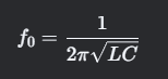
Example: For 2.4 GHz, choose L = 2.2 nH, then C ≈ 2 pF.
Place the LC in shunt (parallel) with the signal path.
At 2.4 GHz, the LC tank creates a low-impedance path to ground, attenuating the signal.
Simulate & Optimize (e.g., in Keysight ADS or Ansys HFSS):
Account for PCB parasitics (trace inductance, via effects).

5. Validation & Tuning
Measure with a Vector Network Analyzer (VNA):
Check S21 (transmission) for rejection depth.
Verify S11 (reflection) for impedance matching.
Adjustments:
Fine-tune L/C values or stub lengths for optimal performance.
Key Challenges in High-Frequency Design
Parasitics: Stray capacitance/inductance shifts f₀.
Component tolerances: Use high-precision parts.
Thermal drift: Select stable materials (e.g., NP0 capacitors).
Final Recommendation
For < 500 MHz: LC filters are practical.
For GHz+ frequencies: Use stub filters or DGS for better performance.
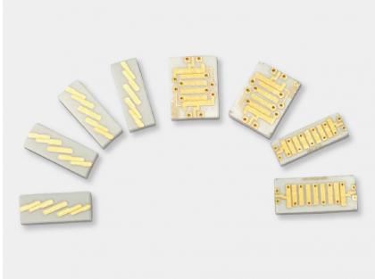
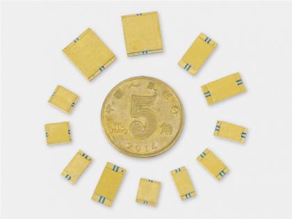
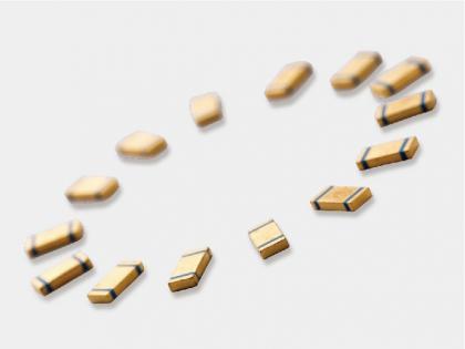
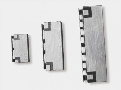
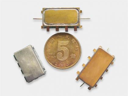
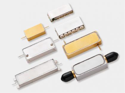
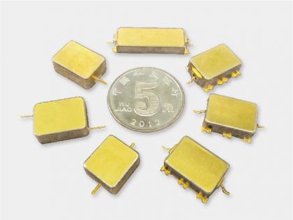
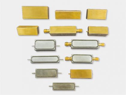
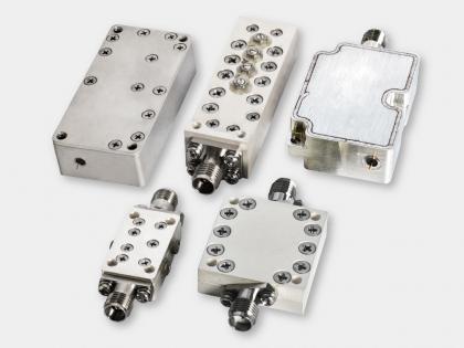
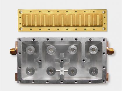
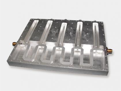
Yun Micro, as the professional manufacturer of rf passive components, can offer the cavity filters up 40GHz,which include band pass filter, low pass filter, high pass filter, band stop filter.
Welcome to contact us: liyong@blmicrowave.com

Address : Xisan Road, Mechanical and Electrical Industrial Park, No.767 Yulan Road, Hefei,Anhui.
Tel : +86-18855146875
Email : liyong@blmicrowave.com


Scan it